💡 Chapter 19: Electronics – Short Questions
Prepared by Muhammad Tayyab, Subject Specialist Physics, Govt Christian High School Daska. Based on PECTAA 2026 syllabus (National Curriculum 2023).
📖 What's Inside: This section covers short questions from Chapter 19 Electronics including semiconductors, doping, PN junction, diode, forward/reverse bias, LED, analog/digital circuits, ADC, DAC, Boolean algebra, logic gates (AND, OR, NOT, NAND, NOR), bit/byte, and fire alarm system. Each question is presented with a precise answer as per the official PECTAA 2026 Physics curriculum. Perfect for Punjab Boards (Lahore, Gujranwala, Multan, etc.) and all BISE boards across Pakistan.
📚 Related Resources – Chapter 19: Electronics
Electronics covers semiconductor devices, diodes, LEDs, logic gates, Boolean algebra, and digital circuits.
📑 Quick Jump to Questions
📝 Short Questions & Answers (PECTAA 2026)
1 Define electronics.
Answer: Electronics is a branch of science that deals with the study and control of the flow of electrons in devices and circuits.
✅ Electronics: Study and control of electron flow in devices and circuits.
2 What is a semiconductor?
Answer: A semiconductor is a material whose electrical conductivity lies between that of conductors and insulators. The most common semiconductors are silicon (Si) and germanium (Ge).
✅ Semiconductor: Conductivity between conductors and insulators.
3 What is doping?
Answer: Doping is the process of adding a small amount of impurity to a semiconductor to increase its electrical conductivity.
✅ Doping: Adding impurities to increase conductivity.
4 What are the two types of doped semiconductors?
Answer: The two types of doped semiconductors are: i. N-type ii. P-type. N-type is formed by adding a pentavalent impurity (e.g., phosphorus). P-type is formed by adding a trivalent impurity (e.g., boron).
✅ N-type and P-type semiconductors.
5 What is a PN junction?
Answer: When an N-type and a P-type semiconductor are joined together, they form a PN junction semiconductor diode.
✅ PN junction: Joining of N-type and P-type semiconductors.
6 What is the depletion region?
Answer: When an N-type and a P-type semiconductor are joined together, electrons from the N-side and holes from the P-side recombine, creating a region without free charge carriers called the depletion region.
✅ Depletion region: Region without free charge carriers at the junction.
7 Why is external voltage applied to a PN junction diode? State the required voltage for silicon and germanium diodes.
Answer: The depletion region acts as a barrier that prevents further movement of charges. To allow current to flow, an external voltage is applied to overcome this barrier. For silicon-based diodes, the required voltage is about 0.7 V, and for germanium-based diodes, it is about 0.3 V.
✅ Silicon: 0.7 V, Germanium: 0.3 V.
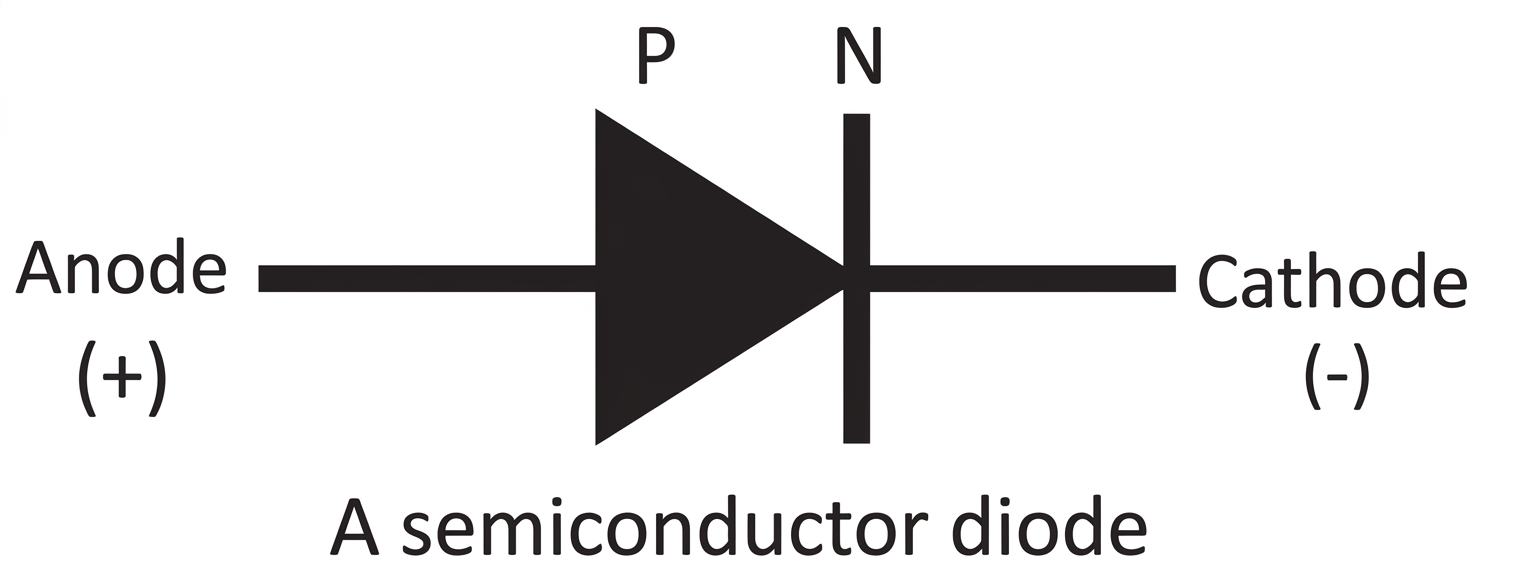
8 What is a semiconductor diode?
Answer: A semiconductor diode is a PN junction device that allows current to flow in only one direction.
✅ Semiconductor diode: PN junction allowing current in one direction.
Symbol:
9 What is forward bias?
Answer: The diode conducts current when the P-side is connected to the positive terminal and the N-side to the negative terminal of a battery. This condition is known as forward bias.
✅ Forward bias: P-side positive, N-side negative.
10 What is reverse bias?
Answer: When the P-side is connected to the negative terminal and the N-side to the positive terminal of a battery, the diode is said to be in reverse bias.
✅ Reverse bias: P-side negative, N-side positive.
11 How does a diode conduct current in forward bias?
Answer: In forward bias, the applied voltage reduces the potential barrier and narrows the depletion region. This allows charge carriers to cross the junction easily.
✅ Reduces barrier, narrows depletion region, allows carrier flow.
12 Why does a small current flow in reverse bias?
Answer: In reverse bias, the depletion region widens, increasing the potential barrier and preventing the flow of majority charge carriers.
✅ Depletion region widens, blocks majority carriers.
13 What is leakage current?
Answer: Leakage current is the very small current that flows in reverse bias due to the movement of minority carriers from both sides of the junction.
✅ Leakage current: Small reverse current due to minority carriers.
14 What does the I-V characteristic curve of a diode show?
Answer: A diode conducts a significant current in forward bias, whereas in reverse bias it blocks the current almost completely.
✅ Forward: conducts; Reverse: blocks.
15 What is an LED?
Answer: A Light-Emitting Diode (LED) is a semiconductor device that allows electric current to flow in one direction, like a typical diode, and emits light when electrons recombine with holes.
✅ LED: Emits light when current flows.
16 How does an LED produce light?
Answer: In forward bias, electrons from the N-type material move across the junction and recombine with holes in the P-type material. Energy is released in the form of photons, producing visible light.
✅ Photons released during recombination.
17 How does an LED work under forward bias?
Answer: When the LED is connected in a forward bias, the applied voltage reduces the depletion region and allows the flow of charge carriers across the junction. Electrons from the N-type material move across and recombine with holes in the P-type material, releasing energy in the form of photons and producing visible light.
✅ Forward bias enables recombination and light emission.
18 Why does an LED work only in forward bias? OR What happens when an LED is connected in reverse bias?
Answer: In forward bias, charge carriers can cross the junction and light is emitted. In reverse bias, the depletion region widens, preventing current flow; therefore, no light is emitted.
✅ Reverse bias: no current, no light.
19 What determines the colour of light produced by an LED?
Answer: The colour of the light produced by an LED depends on the materials used during its manufacture, affecting the wavelength and thus the colour of the emitted light.
✅ Colour depends on semiconductor material.
20 Write any four advantages or applications of LEDs.
Answer: LEDs are highly efficient, durable, energy-saving, and are extensively used in radios, lamps, digital clocks, calculators, video displays, remote controls, and modern lighting systems.
✅ Efficient, durable, energy-saving, widely used.
21 What are analog and digital circuits?
Answer: Analog Circuits: In analog circuits, voltages and currents can vary smoothly and continuously within a certain range. Digital Circuits: In digital circuits, voltages have only two values: "high" (e.g., 5 V) or "low" (e.g., near 0 V).
✅ Analog: continuous; Digital: discrete (high/low).
22 What is an ADC? Why is an ADC needed?
Answer: An analog-to-digital converter (ADC) converts analog signals into digital binary form for processing by computers. Quantities such as sound and light are analog and cannot be directly processed by digital circuits.
✅ ADC: Converts analog to digital for processing.
23 What are the three steps of conversion from analog to digital data?
Answer: The three steps are: 1. Sampling: The continuous analog signal is measured at regular intervals. 2. Quantization: Each sampled value is rounded to the nearest predefined level. 3. Encoding: The quantized values are then converted into binary numbers (0s and 1s).
✅ Sampling, Quantization, Encoding.
24 What is a DAC?
Answer: A digital-to-analog converter (DAC) converts binary data back into an analog signal for output, such as playing sound through a speaker.
✅ DAC: Converts digital to analog for output.
25 What is a binary variable?
Answer: A binary variable has only two possible states, represented by 1 and 0. For example, a switch can be ON (1) or OFF (0).
✅ Binary variable: two states (1 and 0).
26 What is Boolean algebra? What is its importance?
Answer: George Boole developed Boolean algebra, the foundation of digital electronics and computing, which uses binary values (bits), where each bit is either 0 or 1. Boolean algebra is used in ADC and also forms the basis for designing digital systems.
✅ Boolean algebra: Foundation of digital electronics.
27 What is a bit and a byte?
Answer: Bit: A bit is the smallest unit of data in computing and can have either the value 0 or 1. Byte: A byte consists of eight bits and represents data in computers.
✅ Bit: 0 or 1; Byte: 8 bits.
28 Name the three basic Boolean logic operations.
Answer: The three basic Boolean logic operations are AND, OR, and NOT.
✅ AND, OR, NOT.
29 What is a logic gate?
Answer: A logic gate is a basic component of digital circuits that performs logical operations like AND, OR, and NOT. These gates enable digital devices to process binary data and make decisions.
✅ Logic gate: Performs logical operations.
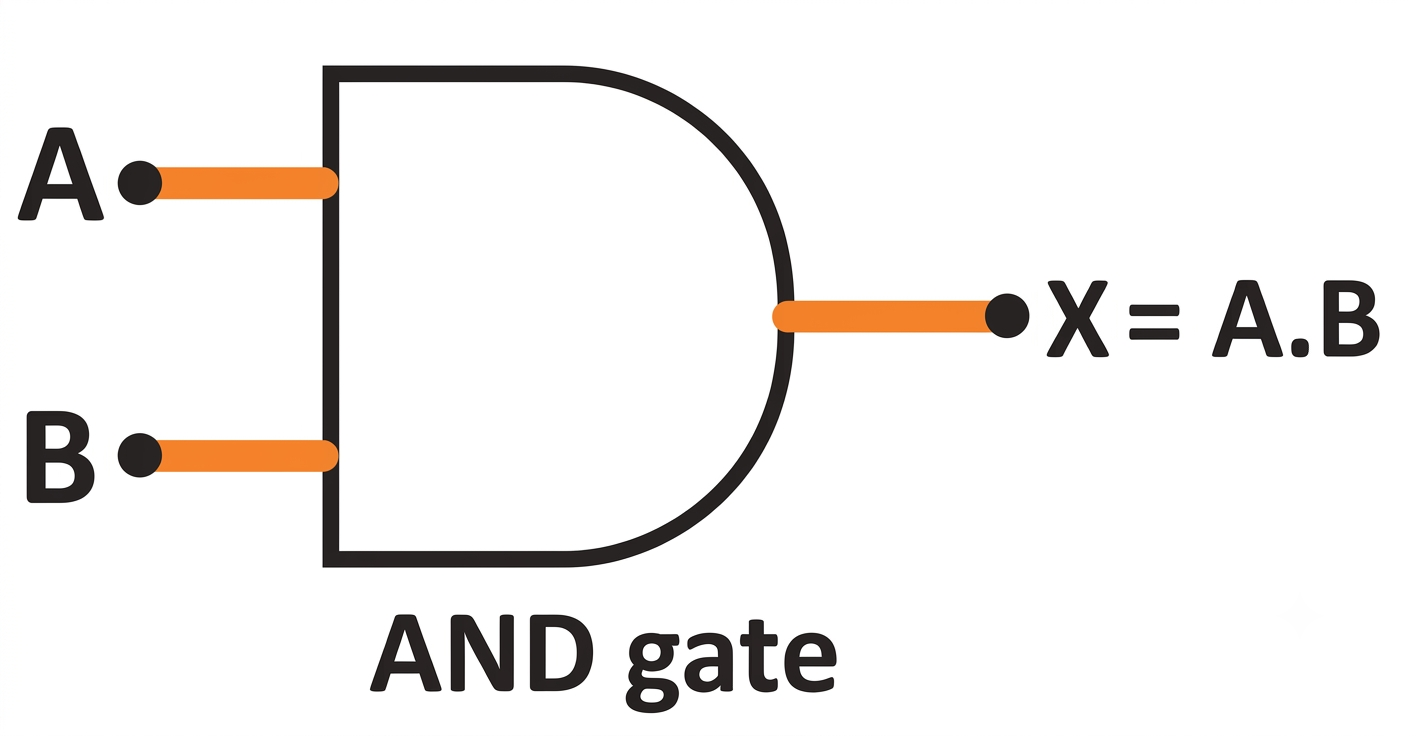
30 What is an AND gate? Also write its logic equation, symbol and truth table.
Answer: AND gate: The AND gate has two inputs. The output of the AND gate will only be 1 (high) if both inputs are 1 (high). In other words, if A and B are two inputs of the AND gate, then output X will be 1 if A = 1 and B = 1.
✅ AND: output 1 only if both inputs are 1.
Logic Equation: \(X = A \cdot B\)
Truth table:
| A | B | X = A · B |
|---|---|---|
| 0 | 0 | 0 |
| 0 | 1 | 0 |
| 1 | 0 | 0 |
| 1 | 1 | 1 |
Symbol:
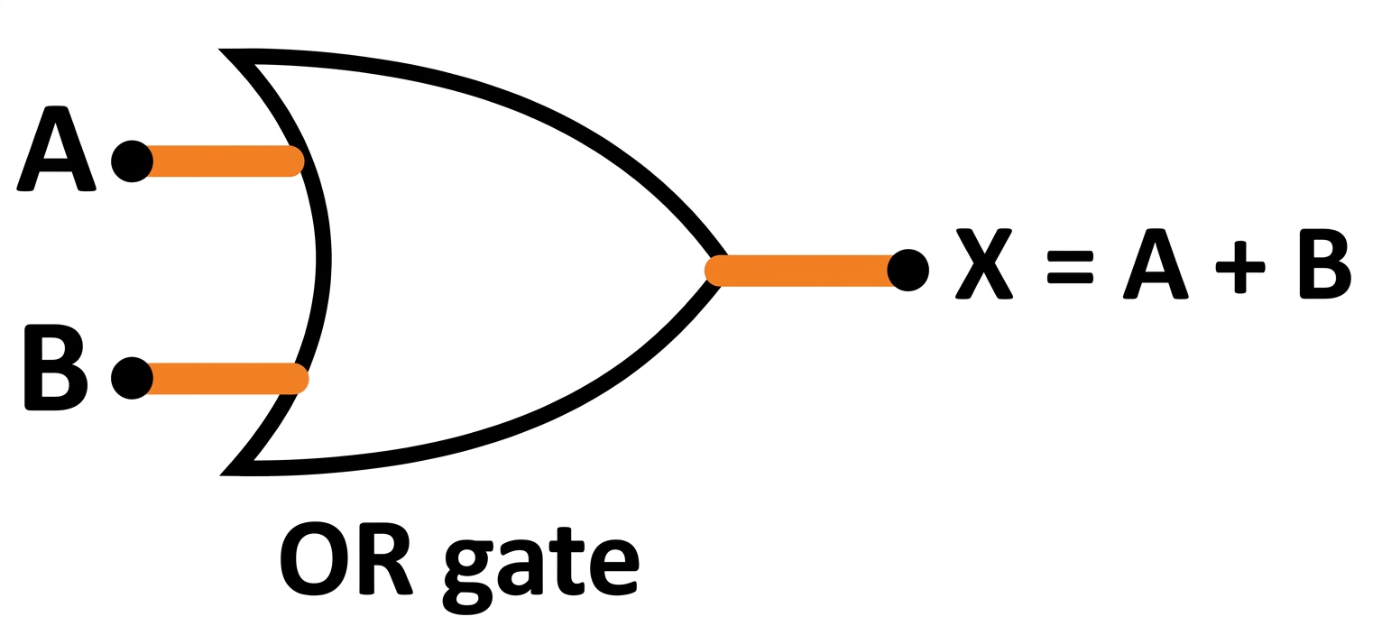
31 What is an OR gate? Also write its logic equation, symbol and truth table.
Answer: OR gate: The OR gate has two inputs. The output of OR gate will be 0 (low) if both the inputs are 0 (low). In other words, if A = 0 and B = 0, then X = 0, otherwise X = 1.
✅ OR: output 1 if at least one input is 1.
Logic Equation: \(X = A + B\)
Truth table:
| A | B | X = A + B |
|---|---|---|
| 0 | 0 | 0 |
| 0 | 1 | 1 |
| 1 | 0 | 1 |
| 1 | 1 | 1 |
Symbol:
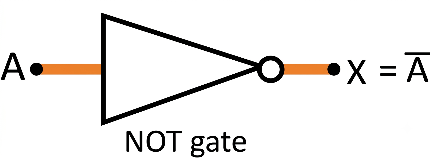
32 What is a NOT gate? Also write its logic equation, symbol and truth table.
Answer: NOT gate: NOT gate has single input. It is also called an inverter as it inverts the input signal, i.e., if its input is 1, then the output will 0 and vice versa.
✅ NOT: Inverts the input.
Logic Equation: \(X = \bar{A}\)
Truth table:
| A | X = Ā |
|---|---|
| 0 | 1 |
| 1 | 0 |
Symbol:
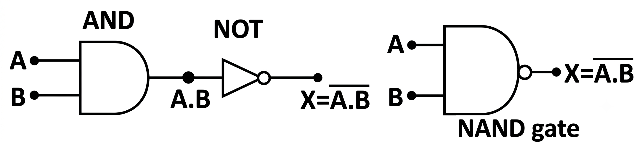
33 What is a NAND gate? Also write its logic equation, symbol and truth table.
Answer: NAND gate: A NAND gate is a combination of AND gate and NOT gate. The output of NAND gate will be 0 when both inputs A and B are 1, otherwise output is 1.
✅ NAND: output 0 only when both inputs are 1.
Logic Equation: \(X = \overline{A \cdot B}\)
Truth table:
| A | B | X = A · B |
|---|---|---|
| 0 | 0 | 1 |
| 0 | 1 | 1 |
| 1 | 0 | 1 |
| 1 | 1 | 0 |
Symbol:
34 What is a NOR gate? Also write its logic equation, symbol and truth table.
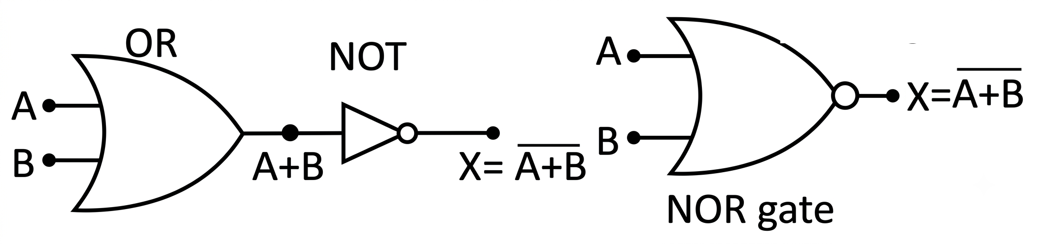
Answer: NOR gate: A NOR gate is an OR gate with a NOT gate at its output. The output of NOR gate will be 1 when both inputs A and B are 0, otherwise output is 0.
✅ NOR: output 1 only when both inputs are 0.
Logic Equation: \(X = \overline{A + B}\)
Truth table:
| A | B | X = A + B |
|---|---|---|
| 0 | 0 | 1 |
| 0 | 1 | 0 |
| 1 | 0 | 0 |
| 1 | 1 | 0 |
Symbol:
35 How does a NAND gate work in a burglar alarm?
Answer: The NAND gate outputs low (0) only when both inputs are high (1); otherwise, it outputs high (1). This means the alarm will sound if either the light is blocked (B = 0), the switch is pressed (A = 0), or both events occur simultaneously.
✅ NAND outputs high unless both inputs are high.
36 What is a fire alarm system?
Answer: A fire alarm system detects fire at an early stage by sensing smoke and heat, triggering an alarm to warn people and provide time to take action.
✅ Fire alarm: detects smoke/heat and triggers alarm.
37 How can fire alarms save lives?
Answer: (i) Early detection saves lives.
✅ Early detection saves lives.
38 Which logic gate is used when either smoke or heat triggers an alarm?
Answer: An OR gate is used because the alarm is triggered when either of the conditions is met. A fire alarm system can process inputs from smoke and heat sensors, triggering the alarm when either smoke is detected or heat is detected.
✅ OR gate: triggers if either smoke or heat is detected.
📐 Key Logic Equations – Electronics
AND Gate: \( X = A \cdot B \)
OR Gate: \( X = A + B \)
NOT Gate: \( X = \bar{A} \)
NAND Gate: \( X = \overline{A \cdot B} \)
NOR Gate: \( X = \overline{A + B} \)
Unit 10Thermal Physics
Unit 11Transfer of Thermal Energy
Unit 12Waves
Unit 13Sound
Unit 14Light
Unit 15Electrostatics
Unit 16Electricity
Unit 17Electromagnetism
Unit 18Electromagnetic Induction & EM Waves
Unit 19✨ Electronics
Unit 20Atomic and Nuclear Physics
Unit 21Space and Environment
📖 Complete syllabus coverage for Class 10 Physics (PECTAA 2026) – Units 10 to 21
💡 Exam Tip:
For short questions, always write precise and to-the-point answers. Use key terms like "semiconductor", "PN junction", "forward bias", "LED", "Boolean algebra", and "logic gates" as they are commonly tested in exams. These questions follow the PECTAA 2026 pattern and are prepared by Subject Specialist Muhammad Tayyab.
Created by Hira Science Academy | Aligned with PECTAA 2026 Syllabus