💡 Chapter 19: Electronics – Long Questions
Prepared by Muhammad Tayyab, Subject Specialist Physics, Govt Christian High School Daska. Based on PECTAA 2026 syllabus (National Curriculum 2023).
📖 What's Inside: This section covers long questions from Chapter 19 Electronics including depletion region changes in forward/reverse bias, LED light production and colour determination, Boolean logic and its importance, logic gates (NAND and OR) with truth tables and symbols, NOR gate working and usage, and burglar alarm design using NAND gate and LDR. Each question is presented with a detailed answer as per the official PECTAA 2026 Physics curriculum. Perfect for Punjab Boards (Lahore, Gujranwala, Multan, etc.) and all BISE boards across Pakistan.
📚 Related Resources – Chapter 19: Electronics
Electronics covers semiconductor devices, diodes, LEDs, logic gates, Boolean algebra, and digital circuits.
📝 Long Questions & Answers (PECTAA 2026)
19.1 Explain how the depletion region of a diode changes in forward and reverse bias. What effect does this have on current flow?
Answer:
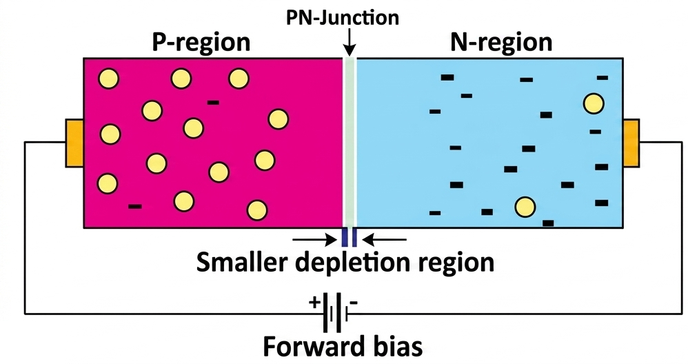
Forward Bias: In forward bias, the P-side is connected to the positive terminal and the N-side to the negative terminal of a battery. The applied voltage reduces the potential barrier at the junction and narrows the depletion region. This enables charge carriers (electrons and holes) to easily cross the junction, causing the flow of current through the diode.
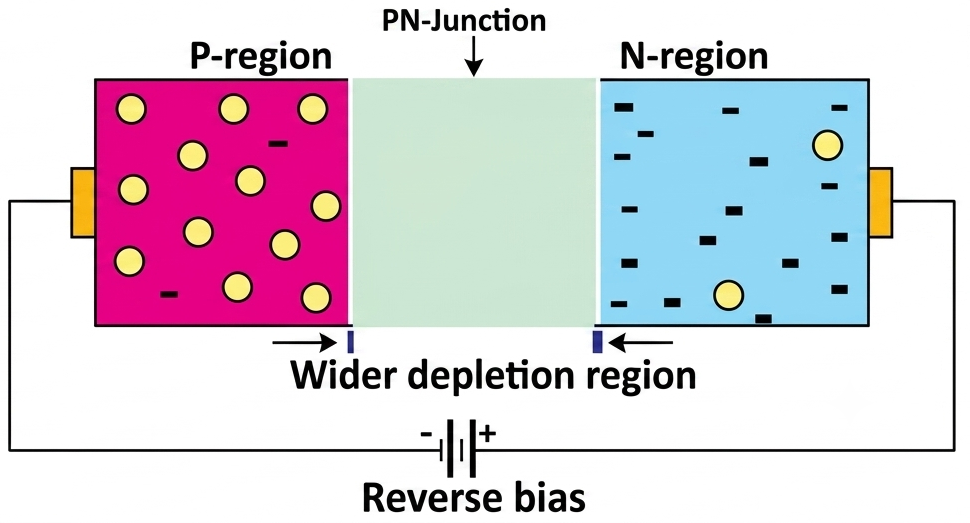
Reverse Bias: In reverse bias, the P-side is connected to the negative terminal and the N-side to the positive terminal of a battery. The depletion region widens, increasing the potential barrier and preventing the flow of majority charge carriers. However, a very small current, known as leakage current, still flows due to the movement of minority carriers from both sides of the junction.
✅ Forward bias: depletion region narrows, current flows. Reverse bias: depletion region widens, current blocked (except leakage).
Forward Bias
Reverse Bias
19.2 Describe how an LED produces light. Also explain how the type of semiconductor material affects the colour of the light.
Answer:
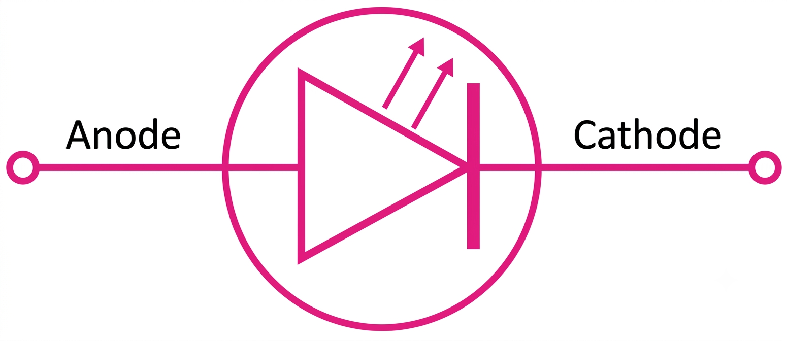
Working of LED: When the LED is connected in a forward bias, the applied voltage reduces the depletion region and allows the flow of charge carriers across the junction. As electrons from the N-type material move across and recombine with holes in the P-type material, energy is released in the form of photons, creating visible light.
Effect of Semiconductor Material: The colour of the light produced by an LED depends on the materials used during its manufacture, affecting the wavelength (and thus the colour) of the emitted light.
✅ LED emits light when electrons recombine with holes. Colour depends on semiconductor material.
LED Symbol:
19.3 What is Boolean logic? Discuss its importance in solving complex digital problems with examples.
Answer:
Boolean Logic: George Boole developed Boolean algebra, the foundation of digital electronics and computing, which uses binary values (bits), where each bit is either 0 or 1. Boolean algebra uses three basic logic operations: AND, OR, and NOT.
Importance: These operations are implemented using logic gates, which are digital circuits with binary inputs and outputs. By using Boolean algebra and logic gates, we can systematically design circuits that process binary data efficiently and reliably. These simple logic gates can be combined to perform complex operations, forming the backbone of modern digital systems.
Examples: For example, an AND gate gives an output of 1 only if all its inputs are 1, while an OR gate gives an output of 1 if at least one input is 1.
✅ Boolean logic: Foundation of digital electronics using AND, OR, NOT. Used to design complex digital systems.
19.4 What are logic gates? Describe the working of NAND and OR gates with the help of truth tables and circuit symbols.
Answer:
Logic Gates: A logic gate is a basic component of digital circuits that performs logical operations like AND, OR, and NOT. Most logic gates have two inputs and one output.
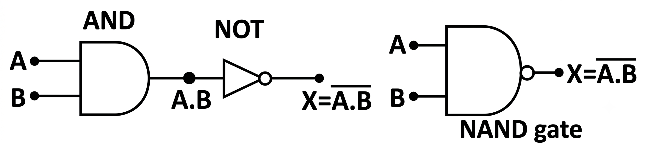
NAND Gate: A NAND gate is a combination of AND gate and NOT gate. The output of NAND gate will be 0 when both inputs A and B are 1, otherwise output is 1.
Logic Equation: \(X = \overline{A \cdot B}\). It is read as \(X\) equals \(A\) AND \(B\) NOT.
Truth table:
| A | B | X = A · B |
|---|---|---|
| 0 | 0 | 1 |
| 0 | 1 | 1 |
| 1 | 0 | 1 |
| 1 | 1 | 0 |
NAND Gate Symbol:
OR Gate: The OR gate has two inputs. The output of OR gate will be 0 (low) if both the inputs are 0 (low). In other words, if \(A = 0\) and \(B = 0\), then \(X = 0\), otherwise \(X = 1\).
Logic Equation: \(X = A + B\). It is read as "\(X\) equals \(A\) OR \(B\)".
Truth table:
| A | B | X = A + B |
|---|---|---|
| 0 | 0 | 0 |
| 0 | 1 | 1 |
| 1 | 0 | 1 |
| 1 | 1 | 1 |
OR Gate Symbol:
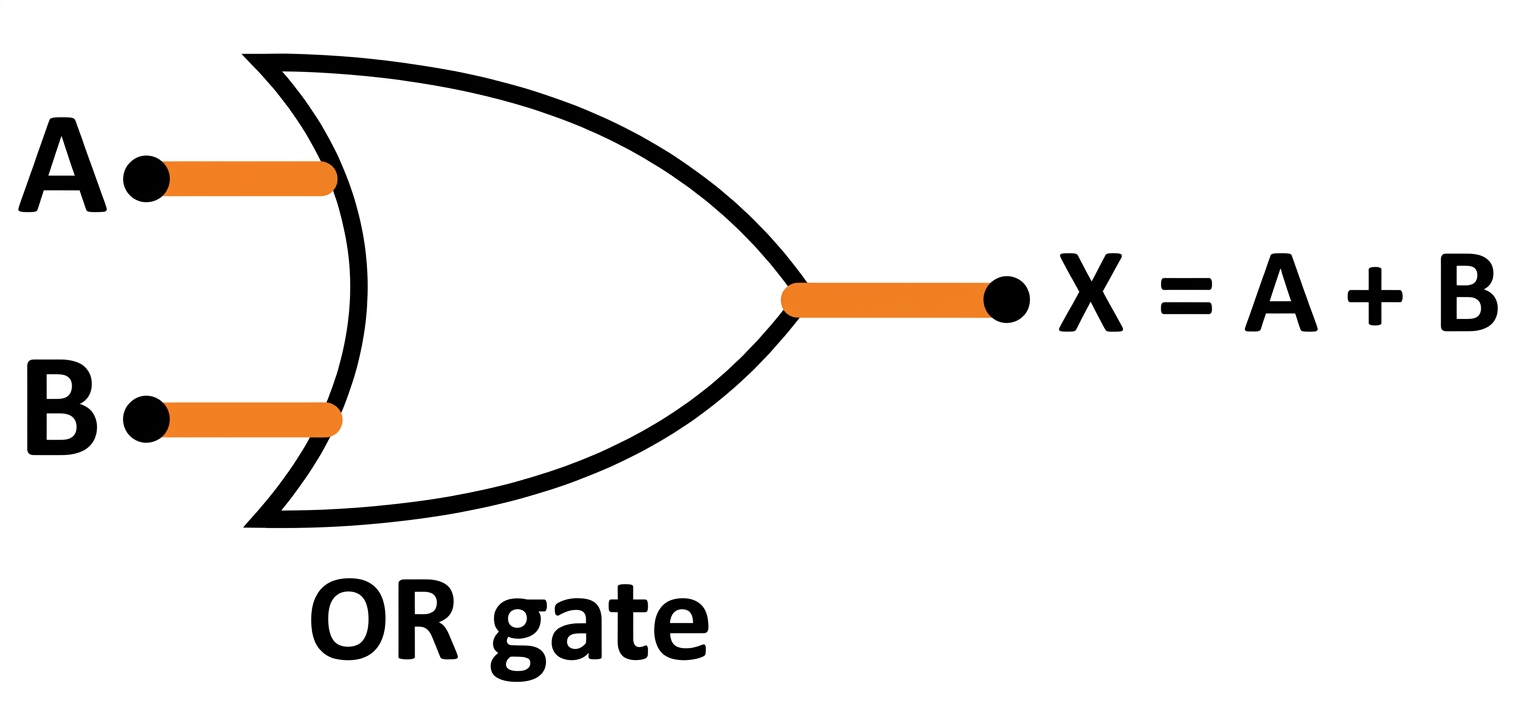
✅ NAND: output 0 only when both inputs are 1. OR: output 0 only when both inputs are 0.
19.5 How does a NOR gate work, and how can it be used to build other basic logic gates?
Answer:
NOR Gate: A NOR gate is an OR gate with a NOT gate at its output. The output of NOR gate will be 1 when both inputs \(A\) and \(B\) are 0, otherwise output is 0.
Logic Equation: \(X = \overline{A + B}\). It is read as \(X\) equals \(A\) OR \(B\) NOT.
Truth table:
| A | B | X = A + B |
|---|---|---|
| 0 | 0 | 1 |
| 0 | 1 | 0 |
| 1 | 0 | 0 |
| 1 | 1 | 0 |
NOR Gate Symbol:
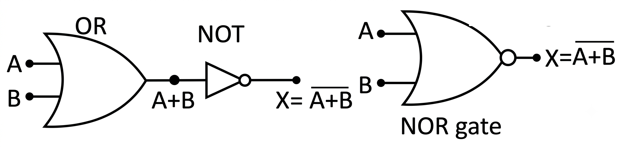
Using NOR Gate to Build Other Gates: NOR gates are universal gates. They can be used to build other basic logic gates:
- NOT gate using NOR: Connect both inputs of the NOR gate together. Output = NOT input.
- OR gate using NOR: Connect the output of a NOR gate to a NOT gate (which is also a NOR gate with inputs tied together).
- AND gate using NOR: Use NOR gates to invert inputs, then feed them into a NOR gate.
✅ NOR: output 1 only when both inputs are 0. Universal gate can build other gates.
19.6 How can a burglar alarm be designed using a NAND gate and an LDR? Explain.
Answer:
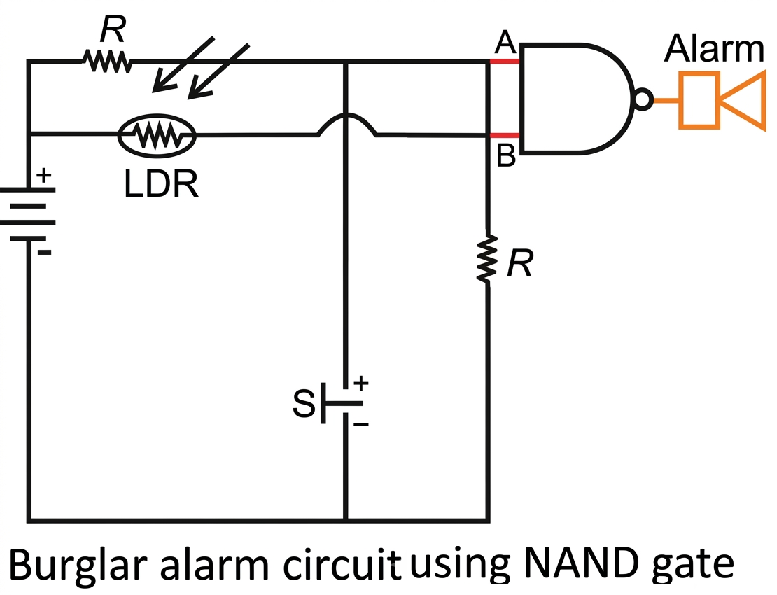
Circuit Connections: We can create a simple burglar alarm using a single NAND gate, an LDR (Light-Dependent Resistor), a push-button switch (S), and an alarm. The LDR is connected between one input (B) of the NAND gate and the positive terminal of the battery, while the push-button switch (S) is connected to the other input (A). The alarm is connected to the output of the NAND gate.
Working: When light falls on the LDR, its resistance is low, causing input \(B\) to be high (1). However, if the burglar interrupts the light, the LDR's resistance becomes high, causing input \(B\) to be low (0). Similarly, if the burglar steps on the push-button switch (S), input \(A\) becomes low (0).
Alarm Activation: The NAND gate outputs low (0) only when both inputs are high (1); otherwise, it outputs high (1). This means the alarm will sound if either the light is blocked (\(B = 0\)), the switch is pressed (\(A = 0\)), or both events occur simultaneously.
✅ NAND gate activates alarm when light is blocked or switch is pressed.
Burglar Alarm Circuit Diagram:
📐 Key Logic Equations – Electronics
NAND Gate: \( X = \overline{A \cdot B} \)
OR Gate: \( X = A + B \)
NOR Gate: \( X = \overline{A + B} \)
Unit 10Thermal Physics
Unit 11Transfer of Thermal Energy
Unit 12Waves
Unit 13Sound
Unit 14Light
Unit 15Electrostatics
Unit 16Electricity
Unit 17Electromagnetism
Unit 18Electromagnetic Induction & EM Waves
Unit 19✨ Electronics
Unit 20Atomic and Nuclear Physics
Unit 21Space and Environment
📖 Complete syllabus coverage for Class 10 Physics (PECTAA 2026) – Units 10 to 21
💡 Exam Tip:
For long questions, write clear and structured answers. Include key terms like "depletion region", "forward bias", "reverse bias", "Boolean algebra", "logic gates", "NAND", "NOR", "LDR", and "burglar alarm". Draw neat logic gate symbols and truth tables for full marks. These questions follow the PECTAA 2026 pattern and are prepared by Subject Specialist Muhammad Tayyab.
Created by Hira Science Academy | Aligned with PECTAA 2026 Syllabus